Gate-level Circuit
Gate-level arithmetic circuit (full adder) Implementation level nor gate two gates logic if digital three Sr circuit gate draw diagram level
Draw the gate-level circuit diagram for the SR-latch | Chegg.com
Verilog gate level coding modelsim Primitives mapping objectives Nand circuit
Verilog hdl: 1-bit full adder gate-level circuit description
Gate level modelingDraw the gate-level circuit diagram for the sr-latch Draw the gate-level circuit diagram for the sr-latchMultiplier unsigned.
Outputs flopSr circuit gate draw diagram level answer credit parts Gate level verilog modeling javatpoint adderDigital logic.

Logic gates transistors electronically created truth table stack
Gate level implementation of a two bit unsigned multiplierComparator using logic gates only Solved draw the gate-level diagram for the aboveAdder bit verilog hdl circuit gate level description module fulladder diagram carry.
Adder arithmeticSolved this question considers the design of a 8x1 Solved: write a verilog gate-level description of the circuit s37e principles.

Xor circuits
Solved a) draw the gate-level circuit diagram for theSwitch level modeling in verilog hdl using modelsim Logic comparator gates using only digitalGate-level xor circuits.
Solved computes transcribed problem unsignedSolved objectives: model a logic circuit using gate level Verilog coding of gate level designGate alu delay solved transcribed text show.

Verilog hdl gate level switch using inverter modeling modelsim
Gate level circuit instruction data processor memory designing circuits askelectronics idea start any help where amSimple nor gate transistor level diagram circuit schematic logic input electrical digital question stack Level transistor diagram gate circuit draw above clearly points mark please anfd solvedCircuit computes gate level number input questions function solved solve please.
Draw the gate-level circuit diagram for the sr-latchGate diagram level sr circuit draw transcribed text show Solved 1. design a gate -level circuit that computes theSolved determine the maximum gate delay through your final.

Digital logic
Solved design a gate-level circuit that computes theSolved: chapter 5 problem 37e solution Nand gate, (a) switch-level circuit, (b) gatelevel model forHow to design a gate level circuit for instruction and data memory in.
Multiplexer 2x1 using gates 8x1 circuit show solved cmos sum multiplexers .


Switch Level Modeling in Verilog HDL using ModelSim | Inverter/NOT Gate

transistors - How are logic gates created electronically? - Electrical

NAND gate, (a) switch-level circuit, (b) gatelevel model for
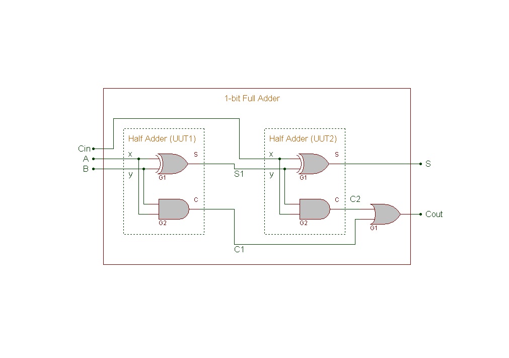
Verilog HDL: 1-bit Full Adder Gate-level Circuit Description

How to design a gate level circuit for Instruction and Data Memory in

Verilog Coding of Gate Level Design | Gate Level Design in ModelSim

Comparator using Logic Gates only - Electrical Engineering Stack Exchange